Electrical interfaces
Power supply
| Pin | Signal |
|---|---|
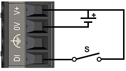
| DI | Digital input #1: +24 VDC ± 20 % (Reference potential is 0V of the device) |
 |
Functional earth (FE, required for EMC) |
| 0V | Reference potential 0 V |
| V+ | Supply voltage +24 VDC ± 20 % |
Schematic diagram for the wiring of digital input no. 1:
Recommendation for use
- The minimum temperature rating of the cables to be connected to the field wiring terminals is 105 °C
- Use flexible cables with a wire cross section of 0.5 mm² / AWG20 and appropriate cable end sleeves.
- To minimise mechanical strain between the individual wires and the plug, the distance between jacket and plug should be at least 30 mm. Recommendation for use: The minimum temperature rating of the cables to be connected to the field wiring terminals is 105 °C Use flexible cables with a wire cross section of 0.5 mm² / AWG20 and appropriate cable end sleeves. To minimise mechanical strain between the individual wires and the plug, the distance between jacket and plug should be at least 30 mm.
Requirements on the power supply
The following requirements also apply to the operation of the digital inputs and outputs:
-
Conformity: Class PS2 acc. to IEC 62368-1 – or – * > *Limited Power Source (LPS) acc. to IEC 60950-1.
-
Voltage: 24 VDC ± 20 %
-
Short-circuit current: \< 8 A
Devices with UL certification for use in the USA and Canada:
The unit and the I/O shall be supplied by an isolated power source which fulfils the requirements of:
-
Limited-Energy Circuit in accordance with UL/CSA 61010-1/ UL/CSA 61010-2-201 or
-
Limited Power Source (LPS) in accordance with UL/CSA 60950-1 or
-
a Class 2 supply source which complies with the National Electrical Code (NEC), NFPA 70, Clause 725.121 and Canadian Electrical Code (CEC), Part I, C22.1.
-
Only use copper conductors to connect the power supply.
Modbus RTU (RS-485)
The fieldbus node is electrically isolated from the power supply of the IRF.
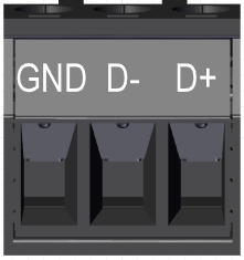 Its electrical bus load is 1/8 unit load (impedance 96 kΩ).
| Pin | Signal |
|---|---|
| GND | Reference potential (common) for the data signals |
| D- | Inverted data signal |
| D+ | Non-inverted data signal |
Recommendation for use
Recommendation: If the device is located at a bus end, a 120 Ω terminating resistor must be attached to the plug between D- and D+ (e.g. a wire resistor covered with heat-shrink tubing).
Digital I/O #2
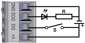
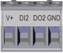
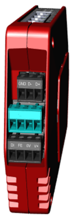 The digital I/O #2 are electrically isolated from the power supply of the device. When operating the digital I/O, the requirements for the power supply according to section 6.1.1 must be observed.
| Pin | Signal |
|---|---|
| V+ | Power supply +24 VDC ± 20 % |
| DI2 | Digital input #2 Current: max. 6 mA Low: 0 … 4.5 V / High: 10 … 30 V |
| DO2 | Digital output #2 Current: max. 0.5 A |
| GND | Reference potential |
Digital I/O #3…5
IRF3801 / IRF3821: 8-pin connector
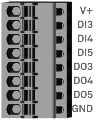
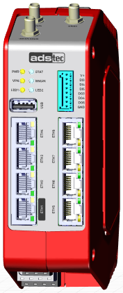 These electrically isolated inputs and outputs are only available with IRF38. When operating the digital I/O, the requirements for the power supply according to section 6.1.1 must be observed. For a schematic diagram: see section 6.3.
| Pin | Signal |
|---|---|
| V+ | Power supply +24 VDC ± 20 % |
| DIx | Digital inputs #3…5 Current: max. 6 mA Low: 0 … 4.5 V / High: 10 … 30 V |
| DOx | Digital outputs #3…5 Current: max. 0.29 A (each) |
| GND | Reference potential |
IRF3851: 12-pin connector (CAN bus and digital I/Os #3…5)
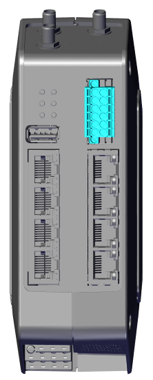
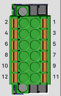
On the IRF3851, the CAN bus and the digital I/Os #3…5 share a common 12-pin connector. Both the CAN bus and the additional digital I/Os are electrically isolated from the power supply of the device and from the other I/Os. If required, the isolation between the I/O groups can be removed by connecting the reference potentials (GND) of the groups together.
When operating the digital I/O, the requirements for the power supply according to section 6.1.1 must be observed.
| Pin | Signal | Description |
|---|---|---|
| 1 | DO.PWR | Power supply for digital outputs +24 VDC ± 20 % |
| 2 | DO.GND | Reference potential for digital inputs and outputs |
| 3 | DO3 | Digital output 3 (max. 0.29 A) |
| 4 | DI3 | Digital input 3 |
| 5 | DO4 | Digital output 4 (max. 0.29 A) |
| 6 | DI4 | Digital input 4 |
| 7 | DO5 | Digital output 5 (max. 0.29 A) |
| 8 | DI5 | Digital input 5 |
| 9 | CAN HIGH | CAN-H data signal |
| 10 | CAN LOW | CAN-L data signal |
| 11 | CAN SHIELD | Shielding |
| 12 | CAN GND | Reference potential |
Digital inputs: Current max. 6 mA / Low: 0 … 4.5 V / High: 10 … 30 V
Recommendation for use
If the device is located at a bus end, a 120 Ω terminating resistor must be attached to the plug between CAN-H and CAN-L (e.g. a wire resistor covered with heat-shrink tubing).
Smart card reader, SIM card and microSD card
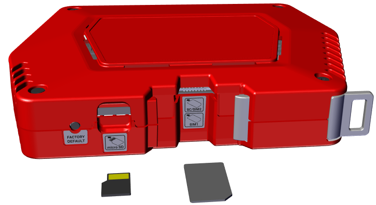
SIM cards and smart cards (SC) in the ID-000 format as defined in ISO 7816 (25x15 mm) can be used.
-
The SIM card for mobile communications must be inserted into the bottom slot (SIM1).
-
The smart card is intended for backing up the configuration data or for connecting to Big-LinX® and must be inserted into the top slot (SC/SIM2).
-
A microSD card with up to 2048 GB can be inserted into the left slot as a memory expansion.
Insert the cards the right way round as shown in the figure:
Recommendation for use
The configuration data of a device can be stored on the smart card. If service is required, the saved configuration can be transferred to the new device. The setup procedure does not need to be repeated.
Recommendation for use
Complex IT infrastructures with a large number of devices can be managed, monitored and controlled easily and conveniently using Big-LinX®. Further information on Big-LinX can be found at: https://www.ads-tec-iit.com/en/reliable-remote-access/biglinx